Semiconductors: The Backbone of Modern Electronics
- May 13, 2025
- 3 min read
Updated: Jul 24, 2025
Semiconductors are the foundation of modern electronics. They power everything from smartphones and laptops to medical devices and electric vehicles. These materials exhibit unique electrical properties that allow them to function as both conductors and insulators. This dual capability enables the creation of complex circuits and microprocessors that drive innovation across nearly every industry.
Challenges in Semiconductor Manufacturing
As semiconductor technologies advance, manufacturers face increasing pressure. They must maintain precision, cleanliness, and reliability throughout the wafer lifecycle. This is critical for ensuring performance and safety in electronic devices. Achilles USA provides specialized wafer handling solutions and semiconductor packaging materials that meet the industry's highest standards for protection, contamination control, and conductivity.
Wafer Packaging Solutions for Safe Transport and Processing
Achilles offers a wide range of wafer packaging products. These products are designed to ensure secure handling throughout each stage of semiconductor manufacturing. Here’s a detailed look:

Horizontal Wafer Shipper (HWS): Our wafer carrier is conductive, clean, and shock-resistant. It protects wafers from risks such as die bond corrosion, electrostatic discharge (ESD), and damage during transportation. Its compact and stackable design ensures efficient wafer shipping.
Single Wafer Shipper: The single wafer shipper is a conductive wafer tray, utilizing our unique technology (ST-poly). It is clean and ESD-protected for safe wafer handling. Due to its high transparency, you can easily view the contents.
Film Frame Shipper (FFS): Achilles' film frame shipper is also conductive, clean, and shock-resistant. It protects wafers from die bond corrosion, ESD, and damage during transportation. This shipper is efficient for shipping wafers with a ring frame, wafer ring, wafer frame, or dicing ring.
Interleaf & Inner Foam: Our wafer spacer and cushion are made from high-quality materials with superior ESD properties. They maintain cleanliness and are compatible with automatic machines for streamlined production.
Benefits of Advanced Wafer Packaging
Effective wafer packaging minimizes risks. Mitigating issues like contamination and physical damage strengthens the reliability of semiconductor devices. Each solution from Achilles is tailored to enhance safety while ensuring performance integrity.
Semiconductor Processing Materials Built for Performance
Beyond packaging, Achilles supports semiconductor production with a selection of high-performance tapes. These are developed specifically for cleanroom and sensitive electronics applications.
Electrostatic Chuck Tape (ESC tape) – Perfect for CVD, sputtering, and plasma etching processes.
Protective Tape – Essential for chemical etching, photolithography, and plating processes.
Heat-resistant Conductive Tape – Available in silicon glue and non-silicon types.
Conductive UV Tape, Conductive Tape, Conductive Thermal Foam Tape – Each designed to enhance performance in delicate procedures.
These products help streamline production. They safeguard delicate materials from physical and electrical damage, ensuring a smooth manufacturing process.
Why Choose Reliable Semiconductor Processing Materials
Using high-quality processing materials accelerates production efficiency. It reduces waste and enhances the durability of the final products. So, opting for Achilles' solutions benefits both the manufacturer and the end-user.
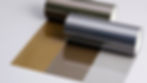
ST-Coating: Advanced Conductive Film Technology
One of Achilles’ standout innovations is its proprietary ST-Coating technology. This conductive coating process enables the development of thin, high-performance conductive materials. The coating retains the shape and texture of the base material.
Conductive films for semiconductors are widely used in applications like HDD parts, circuit protection, and sensitive electronics packaging. ST-Coating provides uniform coating and conductivity on various surfaces.

Key Features of ST-Coating Technology
ESD prevention: Surface resistance: 10^3 Ω < R < 10^8 Ω.
Stable performance: Conductive properties are maintained over time.
High transparency: Approximately 80% light transmittance.
Cleanliness: Low outgassing, low ion contamination, silicon-free.
Heat-resistant: Conductive even when heated to 200°C for 3 minutes.
Your Trusted Partner for Semiconductor Solutions
Achilles’ semiconductor product line is tailored for the complexities of modern electronics manufacturing. We provide everything from precision wafer transport to conductive packaging materials and advanced film technologies. With decades of experience, we are committed to providing high-performance materials.
By choosing Achilles USA, semiconductor manufacturers can improve safety, reliability, and process efficiency.
Contact Achilles USA to learn how our customized solutions can support your wafer handling, processing, or ESD protection requirements. If you want to learn more information about our Semiconductor Transfer and Handling Solutions, access https://www.achilles-semi.com/.
Feel free to reach out to us for any further inquiries or specialized needs in your semiconductor processes. Let’s innovate together!